A key challenge in developing new nanotechnologies is figuring out a fast, low-noise technique for translating small mechanical motions into reasonable electronic signals. Solving this problem will one day make it possible to build electronic signal processing devices that are much more compact than their purely electronic counterparts. Much sooner, it will enable the design of advanced scanning tunneling microscopes that operate hundreds to thousands of times faster than current models.
As exciting as these possibilities are, they aren't the primary driver for research by graduate student Nathan Flowers-Jacobs, former research associate Dan Schmidt, and Fellow Konrad Lehnert on the properties of an atomic point contact displacement detector they designed and built. The researchers want to understand the fundamental physics of the device, which operates in accordance with the laws of quantum mechanics. To accomplish this, they've developed a microwave-based technique to efficiently measure its performance.
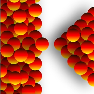
To make the displacement detector, the researchers used lithography tools to create a gold structure with a freely suspended nanomechanical beam (100 nm thick) connected initially to an atomic point contact, as shown below. Then the researchers ran a current through the point, creating an electron wind that shoved atoms aside, creating a tiny gap between the point and the beam. During this process, they measured the resistance of the point contact, looking for a characteristic increase in resistance indicating that electrons had started to hop (tunnel) across the gap. An artist's conception of the atom-sized gap between the atomic point contact and the freely suspended nanomechanical beam is shown at the right.


 The Physics Frontiers Centers (PFC) program supports university-based centers and institutes where the collective efforts of a larger group of individuals can enable transformational advances in the most promising research areas. The program is designed to foster major breakthroughs at the intellectual frontiers of physics by providing needed resources such as combinations of talents, skills, disciplines, and/or specialized infrastructure, not usually available to individual investigators or small groups, in an environment in which the collective efforts of the larger group can be shown to be seminal to promoting significant progress in the science and the education of students. PFCs also include creative, substantive activities aimed at enhancing education, broadening participation of traditionally underrepresented groups, and outreach to the scientific community and general public.